Gear
Gear
News, roundups, and reviews of the technology that shapes the way we live.
Explore Gear
Latest in Gear


Technology
The 50 greatest innovations of 2024

Sponsored Content
There’s one way to make sure you’re never caught unprepared for a storm


Sponsored Content
For the gamer who already has everything—except this

Sponsored Content
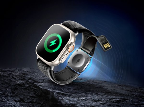
Check out this Apple Watch band charger you didn’t know you needed


Sponsored Content
Capture the holidays in stunning 4K with this drone bundle

Sponsored Content
How Kodak is turning old film into family fun


Sponsored Content
Wow! 68 percent off Microsoft Office during Cyber Week
Sponsored Content