Sponsored Content
Gear
News, roundups, and reviews of the technology that shapes the way we live.
Latest in Gear


Sponsored Content
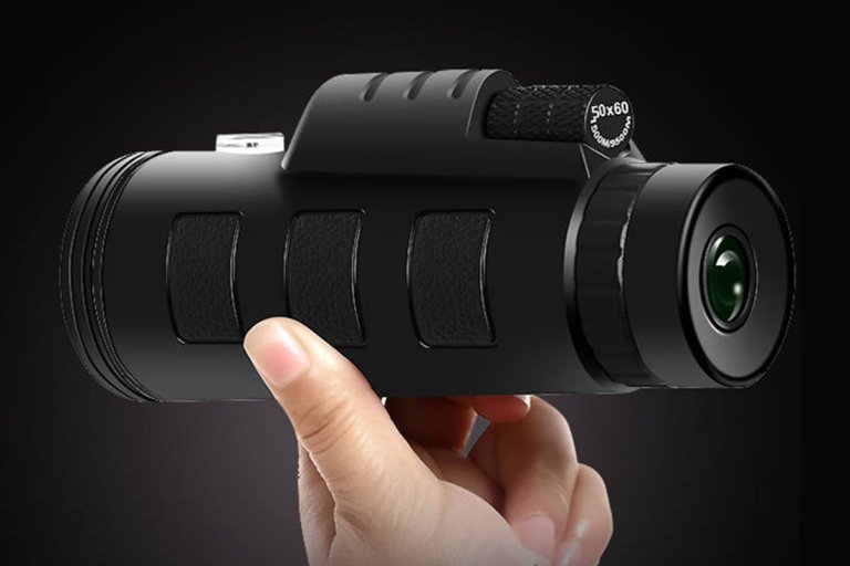
This cool desktop gadget could win you thousands of dollars
Sponsored Content
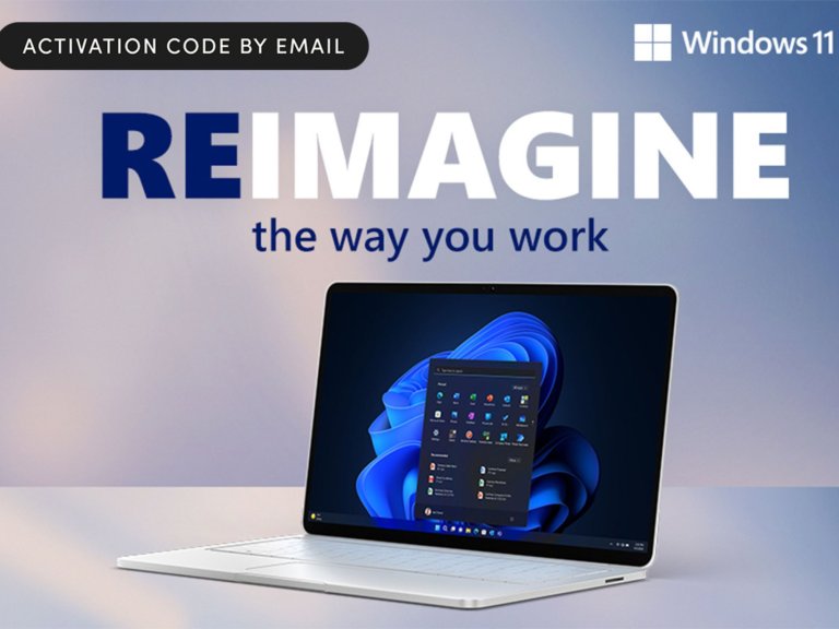
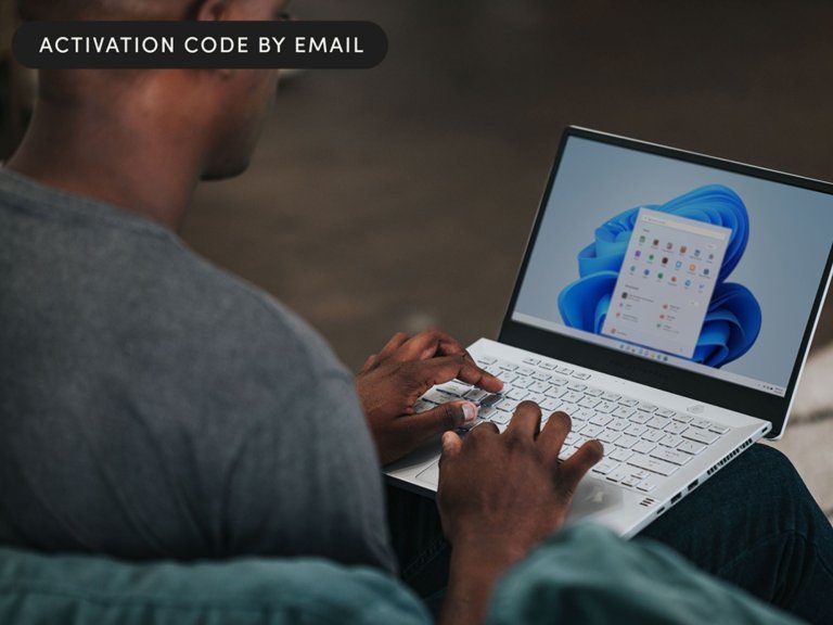
Upgrade to Windows 11 Pro for just $13


Sponsored Content
Start learning ASL today for just $15

Sponsored Content
Spring break is coming — are you sure you’ve gotten the best deal?
Sponsored Content
Say yes to Microsoft Office and no to recurring payments

Sponsored Content
Why buying an air conditioner in winter makes sense (Hint: $100 off)
Sponsored Content
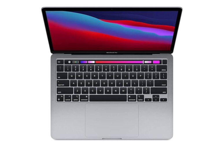
This powerful Apple laptop from 2020 is only $480
Sponsored Content
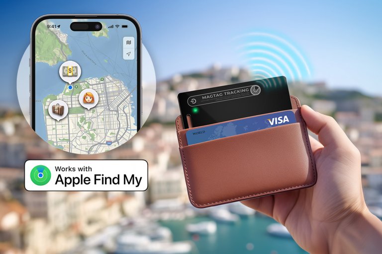
This 1.5mm tracker card fixes the AirTag wallet problem for $24

Sponsored Content
Grinding is optional when lifetime cheats cost $34.99

Sponsored Content
Track snowstorms this winter and beyond for $40

Sponsored Content
Skip the subscriptions—this AI browser copilot is $69 for life

Sponsored Content