First Effective Way to Produce Graphene Sheets Could Usher in the Future of Electronics
Moore’s Law provides the axiom that the number of transistors that can be placed on a circuit will double every...
Moore’s Law provides the axiom that the number of transistors that can be placed on a circuit will double every two years, but as we reach for smaller and smaller tech, silicon and other transistor materials are reaching their physical limits. Lucky for Moore, a European research group has produced graphene of a size and quality that can be practically developed for eventual commercial use.
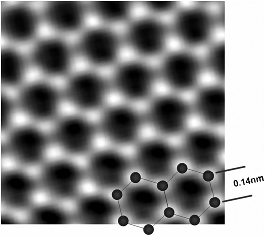
Graphene has been bandied about as a replacement semiconductor material for a while now, but until now, no one has been able to make a decent batch of the stuff that is both large and of sufficient quality — generally it’s been one or the other. At its core, it’s simply carbon arranged in a honeycomb-like layer just a single atom thick. But despite its thinness it’s very conductive and very strong, making it a great candidate material with which to build the next generation of smaller, more powerful electronics.
The researchers were able to create high-quality, high-quantity graphene epitaxially — by growing one crystal layer atop another. By this method, they were able to create a set of graphene layers about 50 square millimeters in area. With this (relatively) large sample, they were able to measure the electrical characteristics of graphene with greater precision than ever before, proving that it indeed has the physical potential to replace conventional semiconductors as the primary building block of future electronics.
Graphene won’t replace normal semiconductors overnight, but the creation of sizeable, high-quality graphene is a significant breakthrough in materials science. Transistors made of graphene should run at higher temps, at faster speeds, and in smaller packages than their semiconductor predecessors, meaning they could maintain the relevance of Moore’s Law for many years to come.