And you thought the macros on your camera was good because you got a sweet close up of a flower? Well, the scientists over at Oak Ridge National Laboratory zoom in so tight they can distinguish atoms of different elements. Using a special z-contrast scanning electron microscope, researchers at Oak Ridge took the first picture detailed enough to differentiate different atoms within a chemical compound. This super-high resolution scanning may play an important role in the future of materials chemistry, where tiny atomic differences can have profound effects on the properties of different chemical compounds.
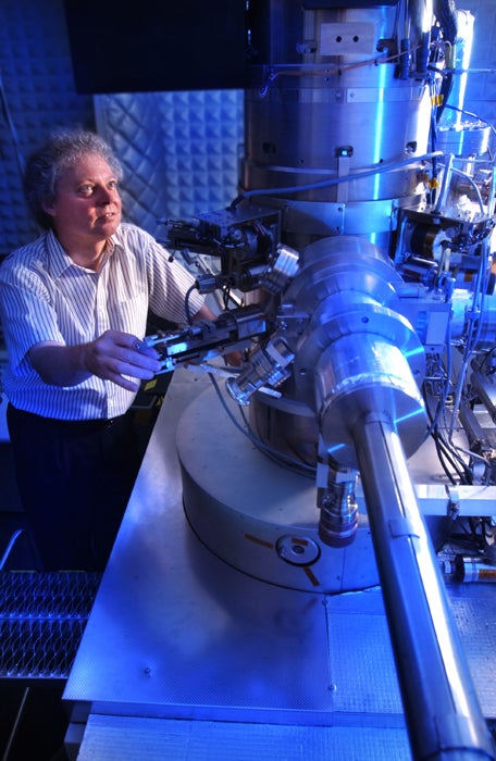
The material in the photo, called boron nitride, consists of boron, nitrogen, and oxygen, with some carbon atoms inserted in place of boron to serve as a control in the image. The electron scanning microscope that took the picture used a 60 kilovolt beam. That's a very low energy for this kind of microscope, because if the beam were any more powerful, it would displace some of the atoms in the compound.
Right now, scientists can only determine the chemical arrangements in a material through chemistry. By developing a technique for taking pictures like this, material chemists and engineers of the future will be able to simple look at the chemical compound to see its geometry and composition.
The incredible innovations, like drone swarms and perpetual flight, bringing aviation into the world of tomorrow. Plus: today's greatest sci-fi writers predict the future, the science behind the summer's biggest blockbusters, a Doctor Who-themed DIY 'bot, the organs you can do without, and much more.


Online Content Director: Suzanne LaBarre | Email
Senior Editor: Paul Adams | Email
Associate Editor: Dan Nosowitz | Email
Assistant Editor: Colin Lecher | Email
Assistant Editor: Rose Pastore | Email
Contributing Writers:
Kelsey D. Atherton | Email
Francie Diep | Email
Shaunacy Ferro | Email
That's what I use for a family portrait!
@StephenD.Alverez
If you didn't have your last name there, I would have asked if you were from the Atoms Family.
I think Stuart must have meant "macro lens" not "macros".
F'ing Amazing
one of the major leaps in modern engineering
F'ing Amazing
one of the major leaps in modern engineering
I'd like to point out that it was scanning transmission electron microscope (STEM) that these images were taken with, NOT scanning electron microscope (SEM). They are different things.
But great work from the folks at Oak Ridge.
Ok.
I always assumed that diagrams of groups of atoms were just mock-ups that were used as a convenient way to explain away the differences between groups of atoms, rather than what scientists actually believed these groups actually look like. I thought atoms would be arranged in a similar
But I'm currently looking at what the Oak Ridge National Laboratory claims is a real image and what I see looks very much like a diagram you'll see in a textbook. It's fuzzy but it appears as if you can even make out the bonds between each atom, which more than anything else I thought just represented the idea of the forces generated by electrons interacting than an actual tangible thing you can look at.
This is really cool, but I want this clarified:
Am I looking at atomic bonds or am I just looking at blurring?
'I thought atoms would be arranged in a similar fashion but not in as exact a fashion as was shown in textbooks.'
That was what I meant to say. I got distracted and thought I wrote it.
I was referring to how the atoms actually are arranged in near perfect hexagons.
SPTNJ07: In a crystalline solid, the atoms are arranged very symmetrically. Naturally, they vibrate somewhat due to heat energy and there are always defects in crystals, but on the average, well crystallized solids can be quite perfectly arranged.
The chemical bonds between atoms are more or less real as well, not just imaginary. When atoms form larger molecules or crystals, the electrons are partially shared between these atoms. Thus there is real electron density between the atoms, aka. "bonds". The actual electron density distribution of course differs from the conceptual "stick" between atoms in chemistry book figures, but still.
Whether the blotches between the atoms in this picture are "bonds" or just blurring is hard to say. Probably both.
It's possible that the connective looking parts between the atoms is just over-lap from the fuzziness of the original image. That or disturbances of the electrons passing through the electron flow between atoms - electrons are being used instead of light for taking the image - it is an electron microscope after all.
Wow - some serious misquoting goof I hope in: "This is not the first picture of... atoms from different elements. However, in those older photos, the atoms were arranged beforehand by scientists."
I took photos of atoms much like this 24 years ago...
www.flickr.com/photos/jurvetson/517311/
And my sample was a regular GaAs lattice, created chemically just like theirs.
While I could not identify atom by atom species, other technology clearly can: atom probe microscopy. It's also 3D. Here are images from 6 years ago!
www.flickr.com/search/?q=atom%20probe&w=44124348109%40N01
Their advance over this is presumably a non-destructive imaging method, which would be useful for various experiments.