How Google’s New A.I. Microchips Take A Page From Bitcoin Miners
Low power specialization, but lots of questions remain...
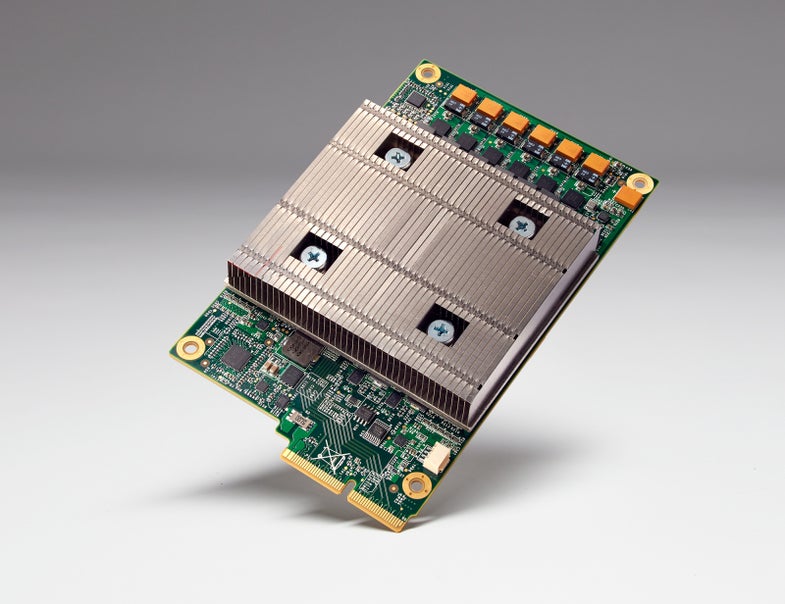
Yesterday at Google’s I/O developers conference, CEO Sundar Pichai briefly spoke about a custom-built chip that helps give Google its edge in machine learning and artificial intelligence. The chip, dubbed a TPU or Tensor Processing Unit (in keeping with Google’s A.I. platform TensorFlow), is specifically wrought for running Google’s decision-making algorithms. Most companies like Facebook and Microsoft use GPUs for their machine learning and artificial intelligence.
But Pichai’s speech and the accompanying blog post only reveal a few details about TPUs. About the only useful thing we know about the chip is that it’s an ASIC, or application-specific integrated circuit. ASIC chips aren’t bought off the shelves, but designed specifically to do one task very well without using a lot of power. They’re used in applications that never change, like the controlling how a phone battery charges.
ASIC designers customize the size and arrangement of the chip’s transistors to closely match the kind of computations needed. Norm Jouppi, a hardware engineer at Google who wrote the TPU blog post, says that the chip was designed to have fewer transistors per operation, because machine learning requires less precise computations.
Pichai’s big statistic is performance per watt—that’s where Google is saying the TPU is an “order of magnitude” better
It’s entirely possible that the TPU chips are simply performing at slightly better speeds, but consuming significantly less power. ASIC chips are extremely power efficient, which is one of the main reasons a recent surge of interest in ASIC chips has been in Bitcoin mining. Mining, like machine learning, requires a computer to quickly perform a large amount of computations and has also typically relied on GPUs.
In the Bitcoin world, an ASIC-based mining rig can consume twenty times less power while doing the same work as a GPU-based rig, as broken down on this Bitcoin forum. In this example, six AMD R9 290 graphics cards (which pull an average of 250 watts each, plus computer components), are stacked against 78 DualMiner ASIC cards (which run off USB and pull 2.5 watts each). Both setups are rated to run the same computations (5.4 Mh/s), but the GPU-based rig conservatively pulls more than 1500 watts while the ASIC rig pulls less than 200 watts.
Basically, the takeaway is that statistics can be misleading, and without seeing objective benchmarks on the TPUs, we should be skeptical of these claims.
ASIC chips have been made since around since the 1960s, and also have some noted downsides. For instance, ASIC chips are designed to run certain code a very specific way. If the machine learning architecture at Google changes, the TPUs could be rendered useless. This is unlikely, as Google uses their Tensorflow platform for everything, but still a possibility.
The Wall Street Journal reports that Google has been using TPUs since April 2015 to speed up how fast Street View reads signs, and Pichai mentioned in his speech that they are being used in Google’s Cloud Machine Learning platform.
Google says they’re not giving any more information about the TPU chips at this time.